
Agent Products/ BRANDS /


X-ray Photoelectron Spectroscopy (XPS) / Electron Probe Microanalyzer (EPMA)X-ray Photoelectron Spectroscopy (XPS) / Electron Probe Microanalyzer (EPMA)
Features and benefits
Instrumentation for surface analysis
Surface chemistry and thin film characterization
Quantitative, chemical identification of the surface
Contact window:sales@scientek-co.com
 / Electron Probe Microanalyzer (EPMA)&name1=brands&pic=scientek_a20201020100240.jpg&prono=b84)
DESCRIPTION
X-ray Photoelectron Spectroscopy (XPS, also known as Electron Spectroscopy for Chemical Analysis – ESCA) is a highly surface-sensitive, quantitative, chemical analysis technique that can be used to solve a wide range of materials problems.
XPS is the measurement of photoelectrons ejected from the surface of a material which has been irradiated with X-rays. The kinetic energy of the emitted photoelectrons is measured, which is directly related to their binding energy within the parent atom; this is characteristic of the element and its chemical state.Only electrons generated near the surface can escape without losing too much energy for detection; this means that XPS data is collected from the top few nanometers of the surface. It is this surface selectivity, coupled with quantitative chemical state identification, that makes XPS so valuable in a vast array of application areas.
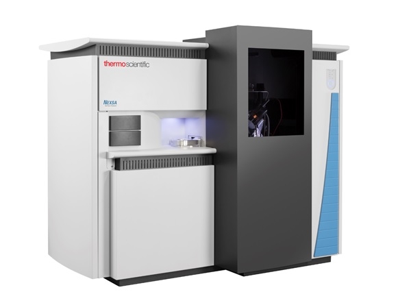
Nexsa XPS system - Unique correlative spectroscopy
High-performance XPS with seamless multi-technique integrationThe Thermo Scientific™ Nexsa™ Surface Analysis system is a fully automated, multi-technique instrument. It features a new, micro-focus X-ray source, delivering both high sensitivity and high spatial resolution XPS. In addition, the system offers options for other surface analysis techniques: UPS, ISS and REELS. Uniquely, there is also the option to integrate a Raman spectrometer, aligned to the XPS analysis position, for true, correlative spectroscopy. With these features, Nexsa unlocks the potential for new insights in semiconductors, 2D materials, thin films, batteries, polymers and many other applications.
• High performance XPS
• Rapid SnapMap XPS imaging
• Depth profiling
• Optional multi-technique integration
––Raman
––ISS
––UPS
––REELS
• MAGCIS ion source for expanded depth profiling capabilities
• Large sample handling
• Avantage Software for instrument control, data processing, and reporting
• Optional transfer capabilities for air-sensitive samples
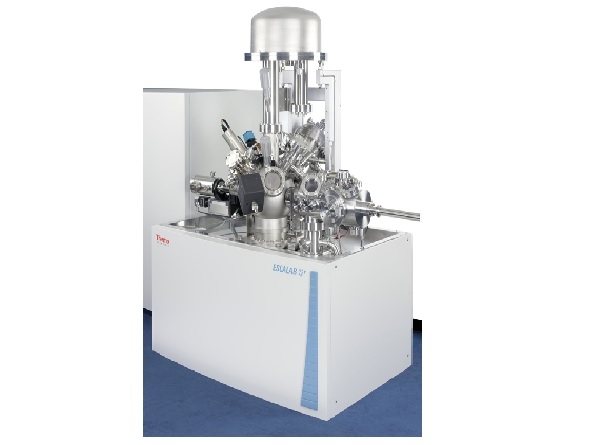
ESCALAB Xi+ XPS microprobe - Performance and versatility
Bringing together high-performance XPS with flexible sample preparationThe Thermo Scientific™ ESCALAB™ Xi+ XPS microprobe is the latest development in our renowned ESCALAB product line. The ESCALAB Xi+ is designed as an expandable, multi-technique platform with unparalleled flexibility and configurability.
System control, data acquisition, processing and
reporting are seamlessly integrated by the powerful
Thermo Scientific™ Avantage™ XPS software
• High-resolution, quantitative XPS imaging for smallest feature analysis
• High-performance spectroscopy
• Ion source for depth profiling
• Flood source for insulator analysis
• Ion scattering spectroscopy (ISS) as standard
• Reflected electron energy loss spectroscopy (REELS) as standard
• Optional additional techniques:
––Ultra-violet photoelectron spectroscopy (UPS)
––Auger electron spectroscopy (AES)
––Microanalysis (EDS)
• Optional MAGCIS dual mode ion source
• Full range of sample preparation options:
––Sample heating and cooling
––Fracture stage
––Inert transfer
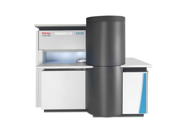
K-Alpha XPS system - Designed for productivity
Making XPS surface analysis routine
The Thermo Scientific™ K-Alpha™ spectrometer bridges the requirements for both research and routine XPS analysis. The high-performance system hardware makes the K-Alpha spectrometer ideally suited to creating world-class data in a busy R&D environment. Intuitive workflows make it possible to put the K-Alpha spectrometer into a multi-user, shared facility, allowing operators of all skill levels to add surface analysis to their materials analysis portfolio.
• High-performance, fully featured XPS system
• Unique sample viewing with capability to facilitate rapid
feature identification
• Chemical state imaging
• Large sample handling
• Variable micro-focus X-ray source to match
analysis area to feature
• Ion source for depth profiling
• Low energy flood source for insulator analysis
• Built-in standards for self-calibration
