
Agent Products/ BRANDS /


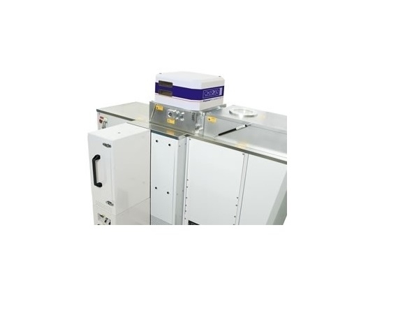
System 100-Plasma Etching and Deposition EquipmentSystem 100-Plasma Etching and Deposition Equipment
Features and benefits This equipment is a flexible and powerful plasma etching and deposition process tool. It adopts a vacuum chamber for quick chip exchange and utilizes various process gases, expanding the permissible temperature range.
Contact window:sales@scientek-co.com
DESCRIPTION
Plasmalab System100 offers maximum process flexibility and is suitable for compound semiconductors, optoelectronics, photonics, MEMS (Micro-Electro-Mechanical Systems), and microfluidic technology. It can be configured in various ways, as detailed below.
Key Features:
- Capable of processing 8" wafers and also offers the ability for small batches (6 × 2") for prototyping and trial production.
- Offers the option of single wafer/batch processing or cassette loading in a vacuum chamber. Plasmalab System100 can be integrated into a cluster system with central robotic wafer handling, allowing for cassette-to-cassette wafer transfer during production. A series of electrodes are used to control substrate temperature, ranging from -150°C to 700°C.
- Laser interferometry and/or optical emission spectroscopy can be installed on the Plasmalab System100 for enhanced etch control.
- Provides the flexibility of selecting 6 or 12 gas boxes for process flow and process gas options. These gas boxes can be placed remotely, away from the main process equipment.
Processes:
Examples of processes using Plasmalab System100 plasma etching and deposition equipment include:
- Low-temperature silicon etching, deep silicon etching, and SOI (Silicon-on-Insulator) processes used in MEMS, microfluidic technology, and photonics.
- III-V semiconductor etching for laser facet processing, etching holes, photonic crystals, and many other applications. The materials range widely and include InP, InSb, InGaAsP, GaAs, AlGaAs, GaN, AlGaN, and more.
- Pre-production and R&D processes for GaN, AlGaN, and others, such as HBLED (High-Brightness Light Emitting Diodes) and other power device etching.
- High-quality, high-rate SiO2 deposition used in photonics devices.
- Metal etching for materials like Nb (Niobium) and W (Tungsten).
