
Agent Products/ BRANDS /


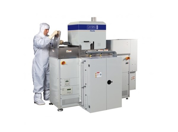


Atomic Layer Deposition System FlexAL ALDAtomic Layer Deposition System FlexAL ALD
Features and benefits Atomic Layer Deposition (ALD) is a true "nano" technology that deposits ultra-thin films of a few nanometers in a precisely controlled manner. Two defining features of atomic layer deposition -- self-confined layer-by-layer growth of atoms and highly conformal coatings -- offer numerous benefits to semiconductor engineering, microelectromechanical systems, and other nanotechnology applications.
DESCRIPTION
Advantages of Atomic Layer Deposition
Because the ALD process deposits precisely one atomic layer per cycle, it enables complete control over the deposition process at the nanometer scale Conformal coating enables even at very high aspect ratios and complex structures enables pinhole and particle-free deposition
Many types of materials can be deposited using ALD:
Oxide,including HfO2, HfSiO, Al2O3, Ta2O5, TiO2, La2O3, SiO2, ZnO
nitride,including TiN, TaN, AlN, SiNx, HfN
metal,including Ru, Cu, W, Mo
Advantages of Remote Plasma Atomic Layer Deposition
In addition to the advantages of thermal ALD, remote plasma allows a wider choice of chemicals used as sources, while also improving film quality:
Plasma enables low-temperature atomic layer deposition processes, and remote sources maintain low plasma damage. More efficient metal source using hydrogen plasma instead of complicated heated source. Eliminates the need for water as a source, reducing the number of cleanings between each ALD cycle—especially at low temperatures. Higher quality films are obtained by further removing impurities, resulting in lower resistivity, higher density, etc.
Ability to control stoichiometry
plasma surface treatment
For some materials, the reaction chamber can be cleaned by plasma
Applications of Atomic Layer Deposition
includes:
High-K Gate Oxide
Energy Storage Capacitor Dielectric
Pinhole-free passivation layers for OLEDs and polymers
Passivation of monocrystalline silicon solar cells
High Aspect Ratio Diffusion Barriers for Cu Interconnects
Adhesive layer
organic semiconductor
Highly Conformal Coatings for Microfluidic and MEMS Applications
Other Nanotechnology and Nanoelectronics Applications
Coating with nanopore structure
Fuel cells, e.g. single technology coatings for catalytic layers
Biological MEMS
