
Product Information/ PRODUCTS /Plasma-Enhanced Chemical Vapor Deposition (PECVD) System for TEOS Multi-Wafer Processing

Plasma-Enhanced Chemical Vapor Deposition (PECVD) System for TEOS Multi-Wafer ProcessingPlasma-Enhanced Chemical Vapor Deposition (PECVD) System for TEOS Multi-Wafer Processing
specification:
The equipment is a flexible and powerful plasma etching and deposition process device. It features a vacuum chamber for fast chip replacement, supports various process gases, and expands the allowable temperature range.
 System for TEOS Multi-Wafer Processing&name1=products&pic=scientek_a20200819110341.jpg&prono=p28)
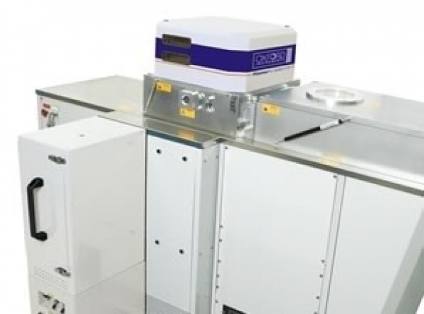
DESCRIPTION
With maximum process flexibility, suitable for compound semiconductors, optoelectronics, photonics, MEMS, and microfluidic technologies, the Plasmalab System100 offers a range of configurations, as detailed below:Key Features:
Capable of handling 8" wafers, as well as small-batch (6 × 2") pre-fabrication and pilot production.
Choice of single-wafer/batch processing or cassette loading in a vacuum chamber.
The Plasmalab System100 can be integrated into a cluster system with central robotic wafer transfer and full cassette-to-cassette wafer transfer in the production process. Substrate temperature control is achieved using a range of electrodes, with a temperature range of -150°C to 700°C.
Laser interferometry and/or optical emission spectroscopy for endpoint detection can be installed in the Plasmalab System100 to enhance etch control.
Optional 6 or 12 gas box configurations offer flexibility in process flow and process gas selection and can be placed remotely, away from the main process equipment.
Processes:
Examples of processes using the Plasmalab System100 plasma etch and deposition equipment include:
Low-temperature silicon etching, deep silicon etching, and SOI processes for applications in MEMS, microfluidics, and photonics.
III-V etching processes for laser facets, photonic crystals, and many other applications, with a wide range of materials (InP, InSb, InGaAsP, GaAs, AlGaAs, GaN, AlGaN, etc.).
Pre-production and R&D processes for GaN, AlGaN, and other materials, such as HBLED and other power devices.
High-quality, high-rate SiO2 deposition for photonic device applications.
Metal (Nb, W) etching.
