
Agent Products/ BRANDS /


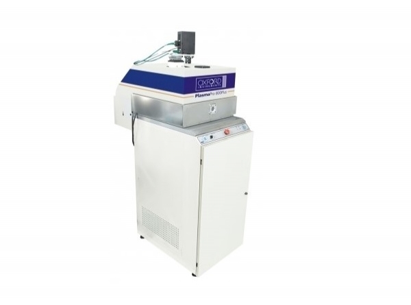


Plasma-Enhanced Chemical Vapor Deposition System (PECVD)Plasma-Enhanced Chemical Vapor Deposition System (PECVD)
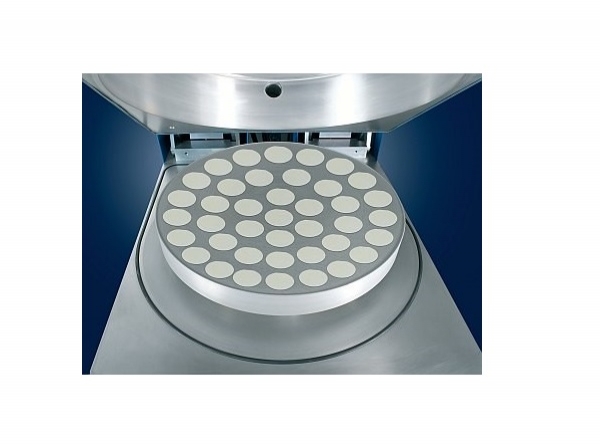
Features and benefitsBatch sizes
| Wafer size | No. Wafers |
|---|---|
| 50mm/2” | > 43 |
| 75mm/3” | 21 |
| 100mm/4” | 12 |
| 150mm/6” | 5 |
| 200mm/8” | 2 |
| 300mm/12” | 1 |
&name1=brands&pic=scientek_a20201019041146.jpg&prono=b45)
DESCRIPTION
Product description
Plasma Enhanced Chemical Vapor Deposition System(PECVD)
main feature
RF driven (megahertz and/or kilohertz) top electrode; no RF bias on bottom (substrate) electrode
The substrate is placed directly on the heating electrode
Gas enters the reaction chamber through a showerhead-style inlet on the top electrode
Working pressure 0.5-1.0 Torr
Power density 0.02-0.1Wcm-2
Advantage
Lower process temperature than traditional chemical vapor deposition
Thin film stress can be controlled by high/low frequency hybrid technology
Plasma dry cleaning process with endpoint control reduces or eliminates the need for physical/chemical cleaning of the reaction chamber
Stoichiometry controlled by process conditions
Provide a wide range of material deposition, including: silicon oxide, silicon nitride and silicon oxynitride deposition, which are widely used in photonic structures, passivation, hard film, etc.
Amorphous silicon(a-Si:H)
Ethyl orthosilicate silica with good step coverage or good step coverage without voids
SiC silicon carbide
diamond-like film
