
Product Information/ PRODUCTS /System 100 -Plasma Etching and Deposition Equipment

System 100 -Plasma Etching and Deposition EquipmentSystem 100 -Plasma Etching and Deposition Equipment
specification:
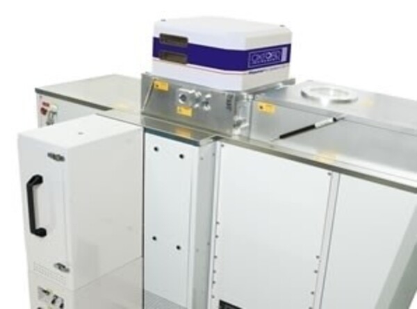
The equipment is a flexible and powerful plasma etching and deposition process device. It adopts a vacuum chamber for sample loading, allowing for quick chip replacement and uses multiple process gases, expanding the permissible temperature range.
With maximum process flexibility, it is suitable for compound semiconductors, optoelectronics, photonics, microelectromechanical systems, and microfluidic technology. The PlasmalabSystem100 can be configured in various ways.
Contact window: sales@scientek-co.com
DESCRIPTION
Main Features:
- Capable of handling 8" wafers and also has the ability for small-batch (6 × 2") pre-processing and trial production.
- Option to choose single-wafer/batch processing or box sampling, carried out in a vacuum chamber. The PlasmalabSystem100 can be integrated into a cluster system with central robotic arm for wafer transfer, and in the production process, full-wafer box-to-box wafer transfer is used.
- Utilizes a series of electrodes for substrate temperature control, with a temperature range from -150°C to 700°C.
- Laser interferometry and/or optical emission spectroscopy can be installed on the Plasmalab System100 for enhanced etching control and endpoint detection.
- The option of 6 or 12 gas boxes provides flexibility in process flow and process gas selection, and can be placed remotely, away from the main process equipment.
Processes:
Here are some examples of processes using Plasmalab System100 for plasma etching and deposition:
- Low-temperature silicon etching, deep silicon etching, and SOI (Silicon-on-Insulator) process, applied in MEMS (Micro-Electro-Mechanical Systems), microfluidic technology, and photonics technology.
- III-V etching processes used for laser diode facet, including etching holes, photonic crystals, and various other applications with a wide range of materials such as InP, InSb, InGaAsP, GaAs, AlGaAs, GaN, AlGaN, and others.
- Pre-production and research and development processes for GaN, AlGaN, etc., including etching for HBLEDs (High-Brightness Light Emitting Diodes) and other power devices.
- High-quality, high-rate SiO2 deposition applied in photonics devices.
- Metal (Nb, W) etching.
